PYNQ is great for accelerating Python applications in programmable logic. Let's take a look at how we can use it with OpenMV camera.
Things used in this project
Hardware:
- Avnet Ultra96-V2 (Can also use V1 or V3)
- OpenMV Cam M7
- Avnet Ultra96 (Can use V1 or V2)
Software:
Introduction
Image processing is required for a range of applications from vision guided robotics to machine vision in industrial applications.
In this project we are going to look at how we can fuse the OpenMV camera with the Ultra96 running PYNQ. This will allow out PYNQ application to offload some image processing to the camera. Doing so will provide a higher performance system and open the Ultra96 using PYNQ to be able to work with the OpenMV ecosystem.
What Is the OpenMV Camera
The OpenMV camera is a low cost machine vision camera which is developed using Python. Thanks to this architecture of the OpenMV Camera we can therefore offload some of the image processing to the camera. Meaning the image frames received by our Ultra96 already have faces identified, eyes tracked or Sobel filtering, it all depends on how we set up the OpenMV Camera.
As the OpenMV camera has been designed to be extensible it provides 10 external IO which can be used to drive external sensors. These 10 are able to support a range of interfaces from UART to SPI, I2C and PWM. Of course the PWM is very useful for driving servos.
On very useful feature of the OpenMV camera is its LEDs mine (OpenMV M7) provides a tri-colour LED which can be used to output Red, Green, Blue and a separate IR LED. As the sensor is IR sensitive this can be useful for low light performance.
 OpenMV Camera
How Does the OpenMV Camera Work
OpenMV Cam uses micro python to control the imager and output frames over the USB link. Micro python is intended for use on micro controllers and is based on Python 3.4. To use the OpenMV camera we need to first generate a micro python script which configures the camera for the given algorithm we wish to implement. We then execute this script by uploading and running it over the USB link.
This means we need some OpenMV APIs and libraries on a host machine to communicate with the OpenMV Camera.
To develop the script we want to be able to ensure it works, which is where the OpenMV IDE comes into its own, this allows us to develop and test the script which we later use in our Ultra96 application.
We can develop this script using either a Windows, MAC or Linux desktop.
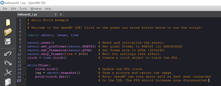
Creating the OpenMV Script using the OpenMV IDE
To get started with the OpenMV IDE we frist need to download and install it. Once it is installed the next step is to connect our OpenMV camera to it using the USB link and then running a script on it.
To get started we can run the example hello world provided, which configures the camera to outputs standard RGB image at QVGA resolution. On the right hand side of the IDE you will be able to see the images output from the camera.
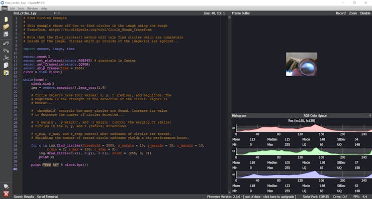
We can use this IDE to develop scripts for the OpenMV camera such as the one below which detects and identifies circles in the captured image.
Note the frame rate is lower when the camera is connected to the IDE.
We can use the scripts developed here in our Ultra96 PYNQ implementation let's take a look at how we set up the Ultra96 and PYNQ
Setting Up the Ultra96 PYNQ Image
The first thing we need to do if we have not already done it, is to download and create a PYNQ SD Card so we can run the PYNQ framework on the Ultra96.
As we want to use the Xilinx image processing overlay we should download the Ultra96 PYNQ v2.3 image.
Once you have this image creating a SD Card is very simple, extract the ISO image from the compressed file and write it to a SD Card. To write the ISO image to the SD Card we need a program such a etcher or win32 disk imager.
With a SD Card available we can then boot the Ultra96 and connect to the PYNQ framework using either
- Use a USB Ethernet connection over the MicroUSB (upstream USB connection).
- Connect via WiFi.
- Use the Ultra96 as a single-board computer and connect a monitor, keyboard and mouse.
For this project I used the USB Ethernet connection.
The next thing to do is to ensure we have the necessary overlays to be able to accelerate image processing functions into the programmable logic. To to this we need to install the PYNQ computer vision overlay.
Downloading the Image Processing Overlay
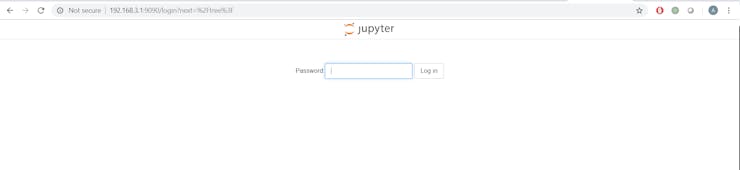
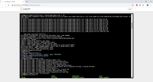
Installing this overlay is very straight forward. Open a browser window and connect to the web address of 192.168.3.1 (USB Ethernet address). This will open a log in page to the Jupyter notebooks, the password is Xilinx
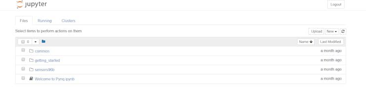
Upon log in you will see the following folders and scripts
Jupyter Initial Files and notebooks
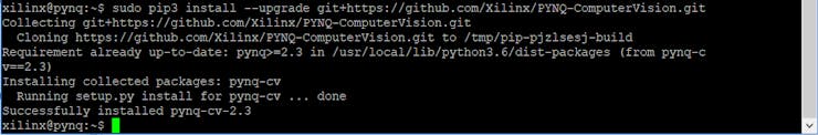
Click on new and select terminal, this will open a new terminal window in a browser window. To download and use the PYNQ Computer Vision overlays we enter the following command
sudo pip3 install --upgrade git+https://github.com/Xilinx/PYNQ-ComputerVision.git
Downloading the PYNQ computer Vision overlays
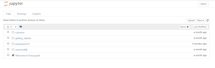
Once these are downloaded if you look back at the Jupyter home page you will see a new directory called pynqOpenCV.
Using these Jupyter notebooks we can test the image processing performance when we accelerate OpenCV functions into the programmable logic.
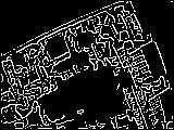
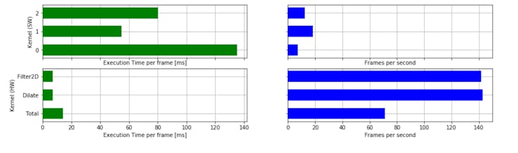
2D filter performance when implemented in HW and SW
Typically the hardware acceleration as can be seen in the image above greatly out performs implementing the algorithm in SW.
Of course we can call this overlay from our own Jupyter notebooks
Setting Up the OpenMV Camera in PYNQ
The next step is to configure the Ultra96 PYNQ instance to be able to control the OpenMV camera using its APIs. We can obtain these by downloading the OpenMV git repo using the command below in a terminal window on the Ultra96.
git clone https://github.com/openmv/openmv
Downloading the OpenMV Git Repo
Once this is downloaded we need to move the file pyopenmv.py
From openmv/tools
To /usr/lib/python3.6
This will allow us to control the OpenMV camera from within our Jupyter applications.
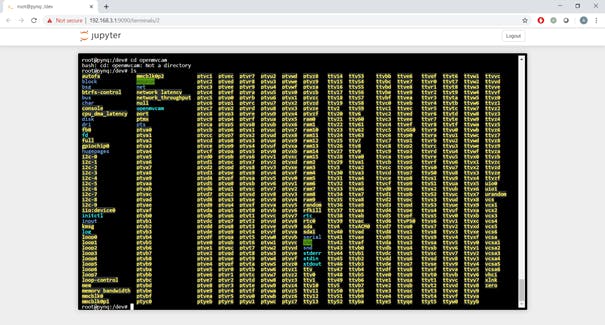
To be able to do this we need to know which serial port the OpenMV camera enumerates as. This will generally be ttyACM0 or ttyACM1 we can find this out by doing a LS of the /dev directory
Now we are ready to begin working with the OpenMV camera in our applications let's take a look at how we set it up our Jupyter Scripts
Initial Test of OpenMV Camera
The first thing we need to do in a new Jupyter notebook is to import the necessary packages. This includes the pyopenmv as we just installed.
We will alos be importing numpy as the image is returned as a numpy array so that we can display it using numpy functionality.
import pyopenmvimport timeimport sysimport numpy as np
The first thing we need to do is define the script we developed in the IDE, for the "first light" with the PYNQ and OpenMV we will use the hello world script to obtain a simple image.
script = """
# Hello World Example
#
# Welcome to the OpenMV IDE! Click on the green run arrow button below to run the script!
import sensor, image, time
import pyb
sensor.reset() # Reset and initialize the sensor.
sensor.set_pixformat(sensor.RGB565) # Set pixel format to RGB565 (or GRAYSCALE)
sensor.set_framesize(sensor.QVGA) # Set frame size to QVGA (320x240)
sensor.skip_frames(time = 2000) # Wait for settings take effect.
clock = time.clock() # Create a clock object to track the FPS.
red_led = pyb.LED(1)
red_led.off()
red_led.on()
while(True):
clock.tick()
img = sensor.snapshot() # Take a picture and return the image.
"""
Once the script is defined the next thing we need to do is connect to the OpenMV camera and download the script.
portname = "/dev/ttyACM0"
connected = False
pyopenmv.disconnect()
for i in range(10):
try:
# opens CDC port.
# Set small timeout when connecting
pyopenmv.init(portname, baudrate=921600, timeout=0.050)
connected = True
break
except Exception as e:
connected = False
sleep(0.100)
if not connected:
print ( "Failed to connect to OpenMV's serial port.\n"
"Please install OpenMV's udev rules first:\n"
"sudo cp openmv/udev/50-openmv.rules /etc/udev/rules.d/\n"
"sudo udevadm control --reload-rules\n\n")
sys.exit(1)
# Set higher timeout after connecting for lengthy transfers.
pyopenmv.set_timeout(1*2) # SD Cards can cause big hicups.
pyopenmv.stop_script()
pyopenmv.enable_fb(True)
pyopenmv.exec_script(script)
Finally once the script has been downloaded and is executing, we want to be able to read out the frame buffer. This Cell below reads out the framebuffer and saves it as a jpg file in the PYNQ file system.
running = True
import numpy as np
from PIL import Image
from matplotlib import pyplot as plt
while running:
fb = pyopenmv.fb_dump()
if fb != None:
img = Image.fromarray(fb[2], 'RGB')
img.save("frame.jpg")
img = Image.open("frame.jpg")
img
time.sleep(0.100)
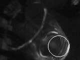
When I ran this script the first light image below was received of me working in my office.
"First Light" from the OpenMV Camera connected to PYNQ environment
Having achieved this the next step is to start working with advanced scripts in the PYNQ Jupyter notebook. using the same approach as above we can redefine scripts which can be used for different processing including
script = """
import sensor, image, time
sensor.reset() # Initialize the camera sensor.
sensor.set_pixformat(sensor.GRAYSCALE) # or sensor.RGB565
sensor.set_framesize(sensor.QQVGA) # or sensor.QVGA (or others)
sensor.skip_frames(time = 2000) # Let new settings take affect.
sensor.set_gainceiling(8)
clock = time.clock() # Tracks FPS.
while(True):
clock.tick() # Track elapsed milliseconds between snapshots().
img = sensor.snapshot() # Take a picture and return the image.
# Use Canny edge detector
img.find_edges(image.EDGE_CANNY, threshold=(50, 80))
# Faster simpler edge detection
#img.find_edges(image.EDGE_SIMPLE, threshold=(100, 255))
print(clock.fps()) # Note: Your OpenMV Cam runs about half as fast while
"""
For Canny edge detection when imaging a MiniZed Board
Alternatively we can also extract key points from images for tracking in subsequent images.
script = """
import sensor, time, image
# Reset sensor
sensor.reset()
# Sensor settings
sensor.set_contrast(3)
sensor.set_gainceiling(16)
sensor.set_framesize(sensor.VGA)
sensor.set_windowing((320, 240))
sensor.set_pixformat(sensor.GRAYSCALE)
sensor.skip_frames(time = 2000)
sensor.set_auto_gain(False, value=100)
def draw_keypoints(img, kpts):
if kpts:
print(kpts)
img.draw_keypoints(kpts)
img = sensor.snapshot()
time.sleep(1000)
kpts1 = None
# NOTE: uncomment to load a keypoints descriptor from file
#kpts1 = image.load_descriptor("/desc.orb")
#img = sensor.snapshot()
#draw_keypoints(img, kpts1)
clock = time.clock()
while (True):
clock.tick()
img = sensor.snapshot()
if (kpts1 == None):
# NOTE: By default find_keypoints returns multi-scale keypoints extracted from an image pyramid.
kpts1 = img.find_keypoints(max_keypoints=150, threshold=10, scale_factor=1.2)
draw_keypoints(img, kpts1)
else:
# NOTE: When extracting keypoints to match the first descriptor, we use normalized=True to extract
# keypoints from the first scale only, which will match one of the scales in the first descriptor.
kpts2 = img.find_keypoints(max_keypoints=150, threshold=10, normalized=True)
if (kpts2):
match = image.match_descriptor(kpts1, kpts2, threshold=85)
if (match.count()>10):
# If we have at least n "good matches"
# Draw bounding rectangle and cross.
img.draw_rectangle(match.rect())
img.draw_cross(match.cx(), match.cy(), size=10)
print(kpts2, "matched:%d dt:%d"%(match.count(), match.theta()))
# NOTE: uncomment if you want to draw the keypoints
#img.draw_keypoints(kpts2, size=KEYPOINTS_SIZE, matched=True)
# Draw FPS
img.draw_string(0, 0, "FPS:%.2f"%(clock.fps()))
"""
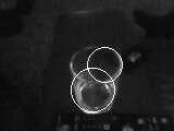
Circle Detection
import sensor, image, time
sensor.reset()
sensor.set_pixformat(sensor.RGB565) # grayscale is faster
sensor.set_framesize(sensor.QQVGA)
sensor.skip_frames(time = 2000)
clock = time.clock()
while(True):
clock.tick()
img = sensor.snapshot().lens_corr(1.8)
# Circle objects have four values: x, y, r (radius), and magnitude. The
# magnitude is the strength of the detection of the circle. Higher is
# better...
# `threshold` controls how many circles are found. Increase its value
# to decrease the number of circles detected...
# `x_margin`, `y_margin`, and `r_margin` control the merging of similar
# circles in the x, y, and r (radius) directions.
# r_min, r_max, and r_step control what radiuses of circles are tested.
# Shrinking the number of tested circle radiuses yields a big performance boost.
for c in img.find_circles(threshold = 2000, x_margin = 10, y_margin = 10, r_margin = 10,
r_min = 2, r_max = 100, r_step = 2):
img.draw_circle(c.x(), c.y(), c.r(), color = (255, 0, 0))
print(c)
print("FPS %f" % clock.fps())
This fusion of ability to offload processing to either the OpenMV camera or the Ultra96 programmable logic running Pynq provides the system designer with maximum flexibility.
Wrap Up
The ability to use the OpenMV camera, coupled with the PYNQ computer vision libraries along with other overlays such as the klaman filter and base overlays. We can implement algorithms which can be used to enable us to implement vision guided robotics. Using the base overlay and the Input Output processors also enables us to communicate with lower level drives, interfaces and other sensors required to implement such a solution.
Originaly posted here.


_LWO95VjQeP.jpeg?auto=compress%2Cformat&w=740&h=555&fit=max)